
Tools
Parts
No parts specified.
-
-
Open KiCAD
-
Create a project by navigating File -> New -> Project
-
Enter your project name in the following box
-
New projects will have 2 associated files
-
.sch - Schematic document. Where you will build the circuit diagram (similar to circuitlab)
-
.kicad_pcb - PCB Layout file. This is where the physical PCB layout and routing will be stored
-
-
-
Click on the schematic layout editor button
-
Alternatively, you can double click on your .sch file
-
The schematic layout editor is where we will define the connections throughout the PCB
-
Later on, the PCB editor will use these connections to draw guide lines for the PCB connections
-
-
-
Navigating the Screen
-
Middle click to pan
-
Scroll wheel to zoom
-
Left click to select (Hold and drag to select multiple components)
-
Left click and drag to move selected components
-
Right click to get other options
-
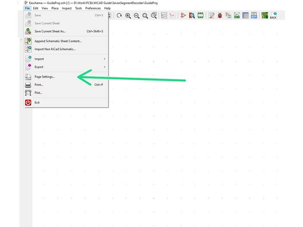
If your design is large, you will want to redefine the schematic area. This step is optional, but will make your schematic look much better.
-
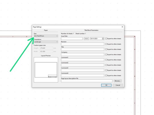
File -> page settings -> Select desired page size. You can also select User(custom) to use any size.
-
-
-
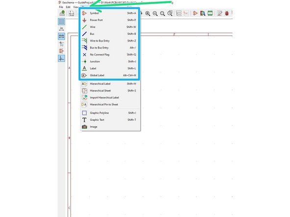
Press the "Place" tab on the top ribbon to begin placing components
-
Select the type of component you want (symbol, power, wire, label)
-
Clicking on the schematic will then place the component.
-
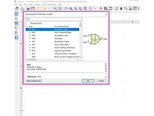
For components, power ports, and labels, this will open a selection screen to choose the component. Double click on the item that you want to place it.
-
For wires, clicking will place the first section of a wire. Clicking into open space will create a junction, and clicking on a component terminal will connect the wire.
-
RIght click and select "wire end" to terminate a wire without a connection.
-
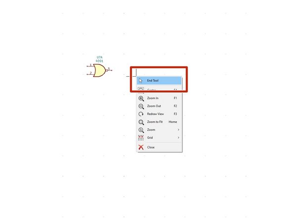
Right click and select "end tool" to stop placing components.
-
-
-
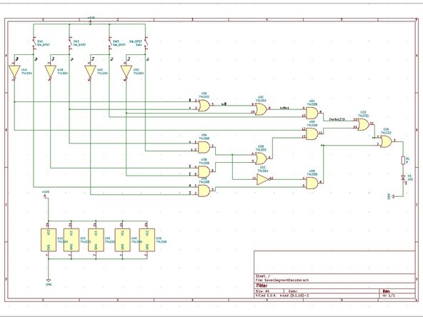
Continue placing components and wires onto the schematic until to complete your design
-
-
-
A footprint is the shape of a PCB component. It is what is actually built into a PCB for the device to be soldered onto
-
Without the right footprint, a component won't fit onto the PCB and won't be able to work in the circuit. If you don't know what footprint to use for a component, the internet is an incredible source
-
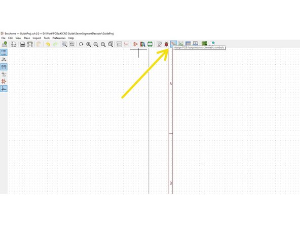
To assign footprints, click "Assign footprints to schematic symbols" on the top ribbon
-
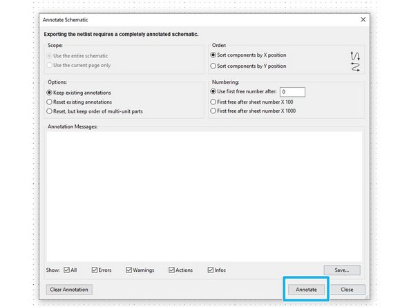
This may bring up a popup saying "Exporting the netlist requires a completely annotated schematic". Pressing the annotate button will add annotations and continue to footprint assignment
-
Annotations are a letter and number combination that are used to define what each component on the board is and reference its position. They are also used to define which gates are being used on a multi-gate integrated circuit
-
You should now be in the footprint assignment menu. This menu has three sections: on the left is the footprint categories, in the center are the components on the schematic, and on the right are a filtered set of footprints (based on what you selected on the left side)
-
To assign a footprint, select a category from the left side, click on the component you want to assign it to, and then double click on the specific footprint you want to use.
-
Repeat for each component on the schematic!
-
-
-
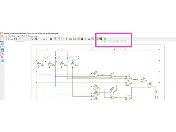
Now that your schematic is built and footprints are assigned, we can design the physical PCB
-
Press the "run pcbnew to layout printed circuitboard button"
-
This will open the PCB layout editor and import your schematic
-
There may be some errors here if you have not defined a footprint for every component in the schematic (missing footprints will be listed)
-
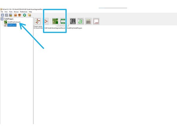
To open the PCB layout editor subsequent times, click on the "Open PCB layout editor" button or double click on your .kicad_pcb file
-
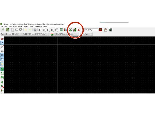
To reupdate the PCB with any changes made to the schematic, press the "Update PCB from schematic" button on the top ribbon
-
-
-
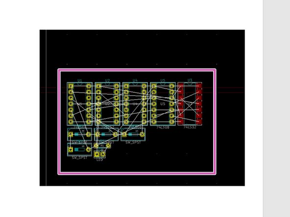
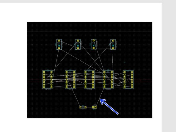
When the PCB is generated, your components will be arranged similarly to this.
-
Left click on a component and drag it to the position you want on the board
-
The white lines show each of the connections from your schematic, so they will move around as the components are arranged.
-
Don't worry if you don't arrange the board perfectly right away, you can always change things later
-
-
-
Here's a quick rundown of the Terminology we will use when laying out a PCB
-
Component/ Device: Anything that goes onto a PCB. Could be a Resistor, Integrated Circuit, Pin Connection, or many other things
-
Trace: A Section of the PCB with copper that connects components
-
Layer: A sheet of copper containing traces. Basic PCBs will have 2 layers, while more complex PCBs typically have anywhere from 3 to 8 layers.
-
Via: Small hole in the board that passes electricity across PCB layers. This allows for traces to "cross" and more complex designs to be made.
-
Gerber Files: Files used to manufacture PCBs. They consist of many different "layers" that define what operations should be done on the PCB.
-
-
-
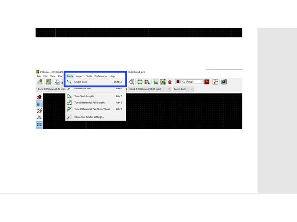
To route traces, select Route -> Single Track.
-
The next place that you click will become the start of a trace. Moving the mouse will cause the software to find the fastest available route from the starting component to the ending component.
-
Clicking in empty space will create a point that the trace must pass through
-
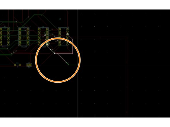
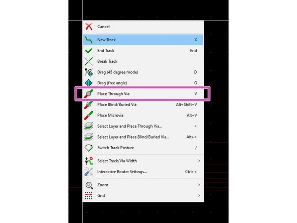
Eventually, there will be no more room on the front of the board. Right click and select "Place Through Via."
-
The next place that you click will create a via and turn the trace green. This is a trace routing on the other side of the PCB!
-
-
-
Now we need to define the edges of the PCB
-
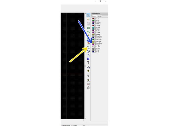
On the right side of the screen, select the "Edge.cuts" layer
-
Once this layer is selected, select the "add graphic lines" button
-
Click and draw to define the footprint of the PCB
-
-
-
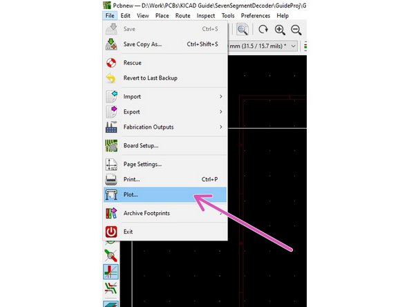
Starting in the PCB Layout editor, enter the plotting menu
-
File -> Plot
-
Make sure that the following layers are selected: Top Copper (F.Cu)+ Soldermask (F.Mask) + Silkscreen (F.SilkS) Bottom Copper (B.Cu) + Soldermask (B.Mask) + Silkscreen (B.SilkS) Board outline (Edge.Cuts)
-
These are the most basic required layers for the PCB. For more complex boards, more layers may be used
-
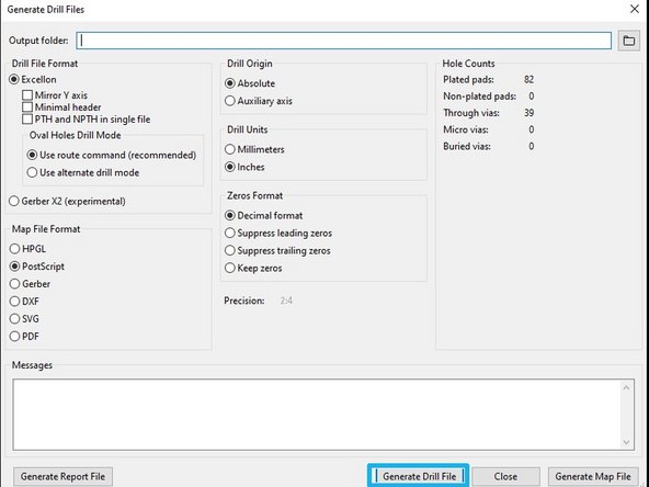
Generate the Drill Files (Default settings are fine)
-
Press the Plot button to generate the gerber file!
-
-
-
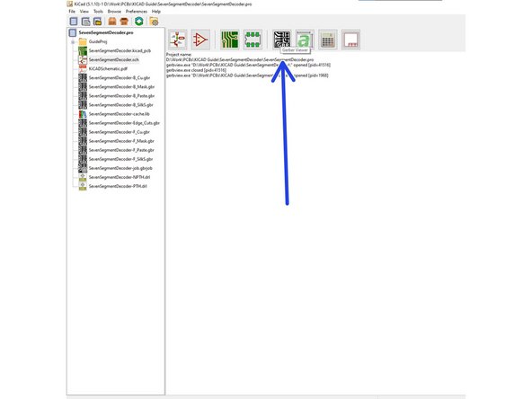
Click on the gerber viewer from the main page
-
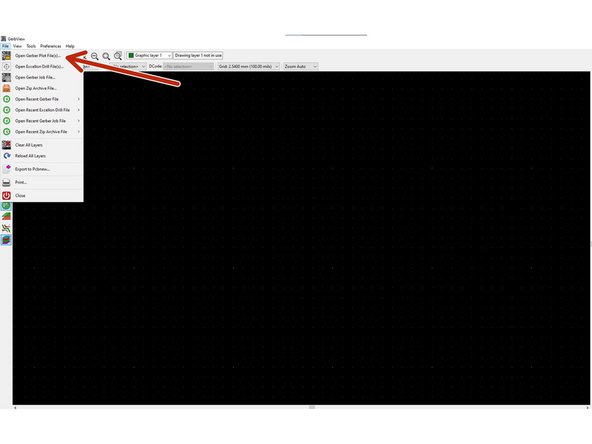
Select file -> open Gerber plot files
-
Select all of the gerber files that were just generated
-
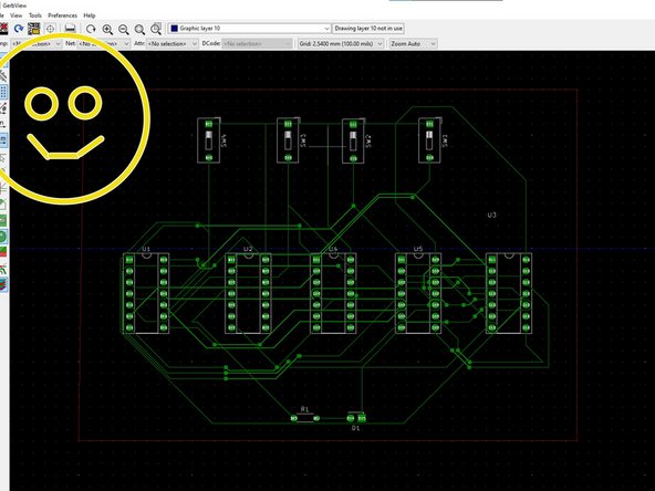
Admire your beautiful new PCB!
-


Cancel: I did not complete this guide.
8 other people completed this guide.