Introduction
EAGLE is electronic design automation (EDA) software that lets printed circuit board (PCB) designers seamlessly connect schematic diagrams, component placement, PCB routing, and comprehensive library content.
Install Eagle here:
-
-
Eagle schematics and layouts are made up of parts. Each part has a symbol as well as a footprint.
-
Symbols are used for creating a schematic by connected components.
-
Footprints are used for planning the PCB layout after a schematic is completed.
-
-
-
We mentioned how parts and their symbols/footprints are used for schematics and layouts.
-
We don't have to start from scratch when designing PCBs.
-
A lot of common parts are included in free libraries and using them would save you a lot of time.
-
Make sure when using a library, the dot next to the library is green.
-
-
-
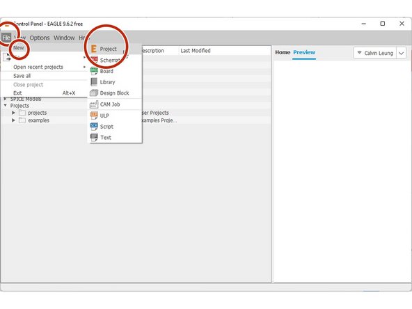
From the control panel: File > New > Project
-
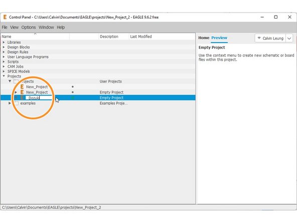
Enter a name for the Project
-
-
-
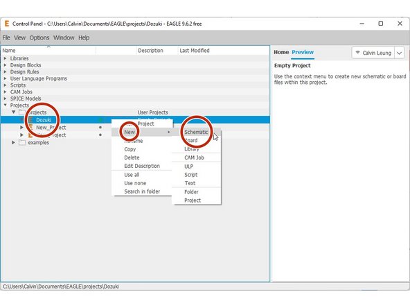
Right-click your project > New > Schematic
-
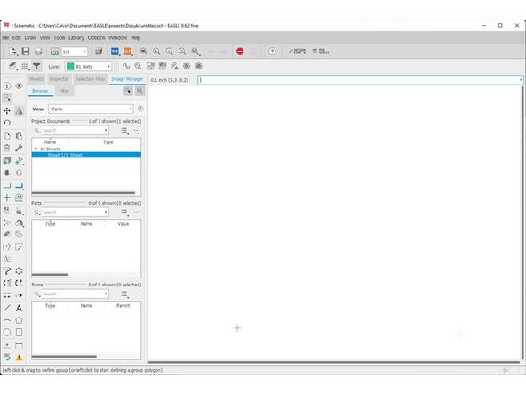
The schematic editor will pop up.
-
Ctrl + s to save and name your schematic
-
-
-
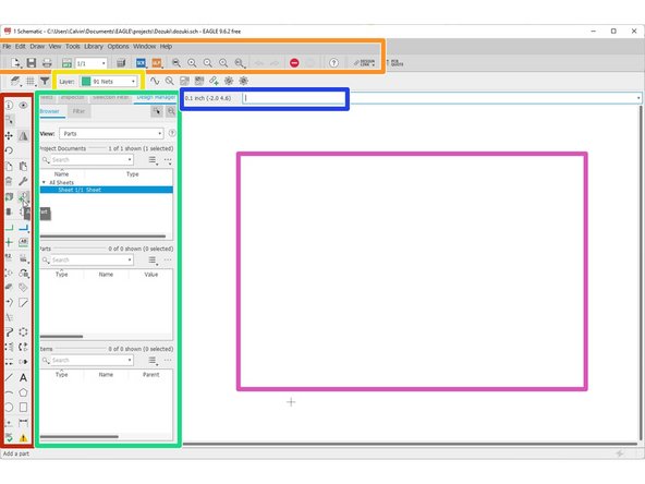
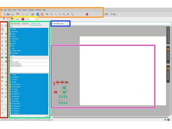
Tool Bar
-
General file control tools
-
Layer
-
Part Properties Editor
-
Command Line
-
Schematic Canvas
-
-
-
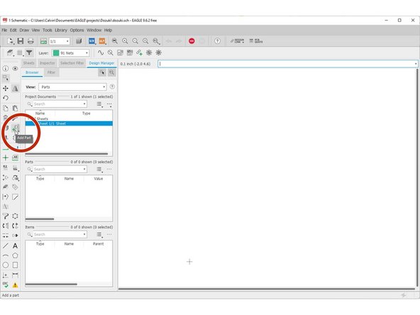
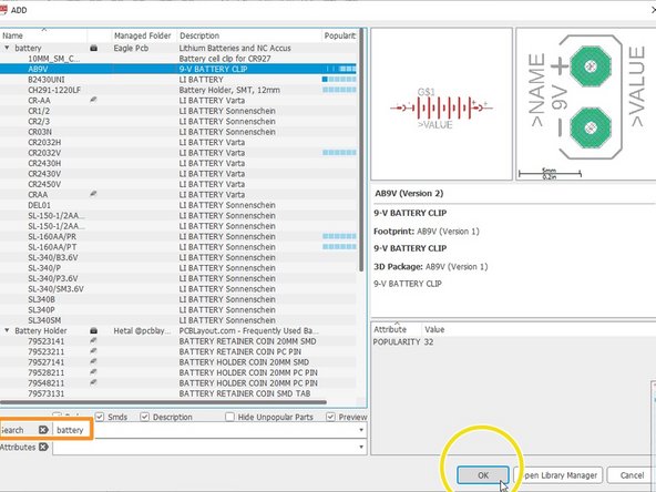
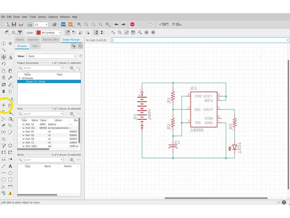
Click "Add Part"
-
Use the Search Bar to look for existing parts in free libraries
-
Click "OK"
-
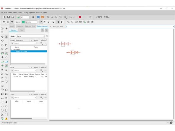
Use left-click to place parts on the schematic
-
Use ESC to stop placing parts
-
-
-
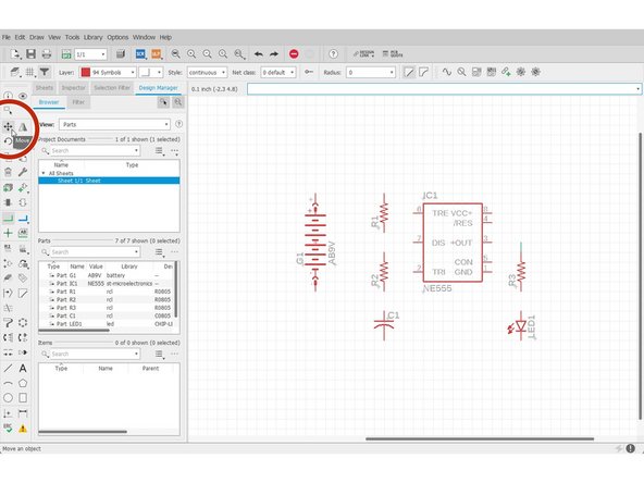
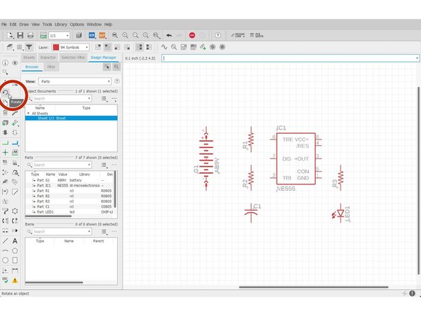
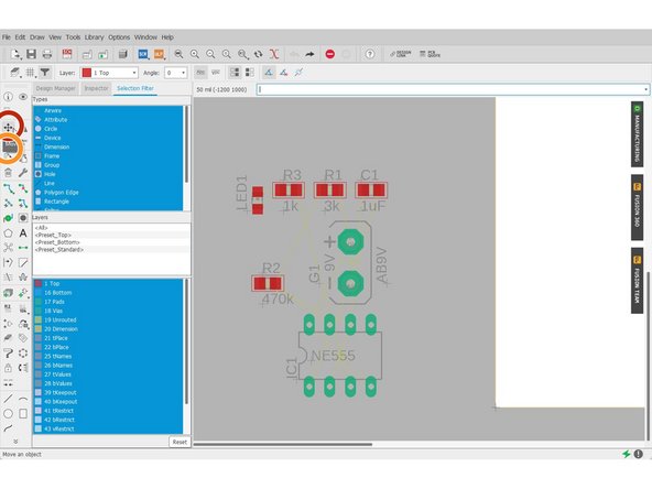
You can oreint your parts with the:
-
Move Tool
-
Rotate Tool
-
-
-
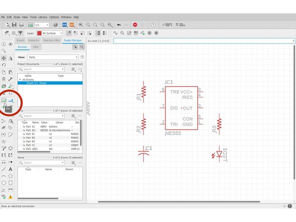
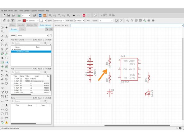
Connect parts with nets.
-
Nets are like wires to connect components together.
-
Select the Nets Tool
-
Make sure you see a circle when initiating a net from one pin to another.
-
Make use of the junction tool when connecting multiple nets.
-
-
-
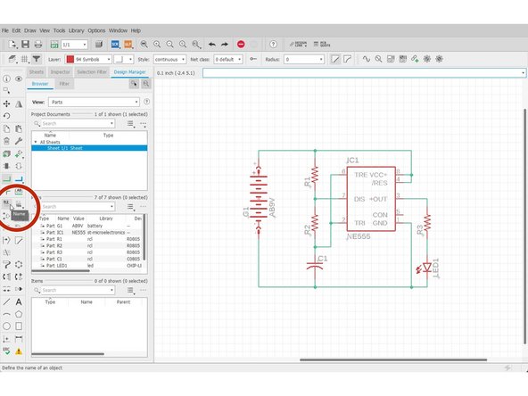
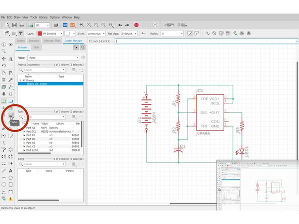
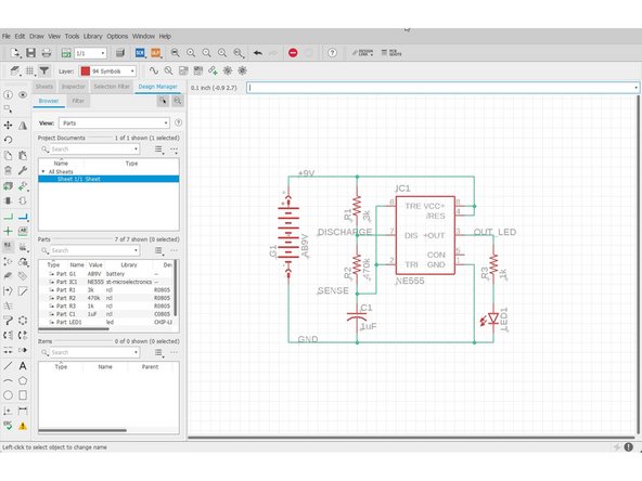
It is important to label parts and nets so that you have the necessary information to make decisions when routing parts.
-
Label Tools such as:
-
Name
-
Value
-
-
-
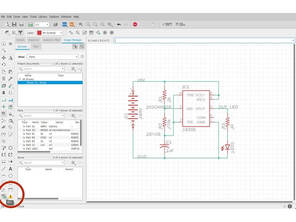
Perform ERC to make sure your schematic is bug-free.
-
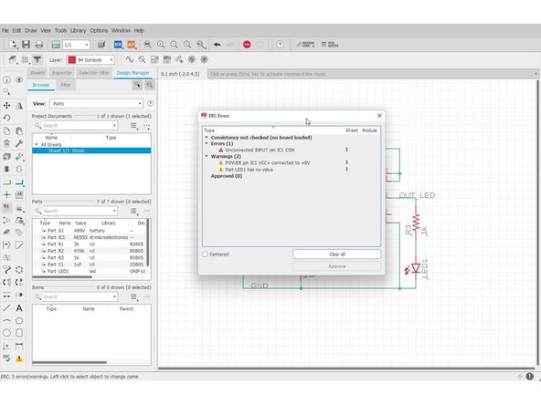
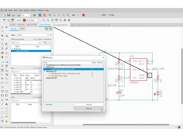
Click "ERC". A list of errors and warnings would pop up. Click individual errors to see where the issue occurs.
-
Errors (1) - These warrant you taking a careful look at. Anything here could very well cause your circuit to fail.
-
Unconnected INPUT pin IC1 CON - In general, unconnected input pins are bad. In this case, the CON pin is a reference voltage that you can manually set, but nothing bad happens if you leave it unconnected (floating).
-
Warnings (2) - These are not as urgent as errors, but still require a cursory glance. One warning to look for is the one about a net only having one node/pin. That means that you didn't connect that net on both ends.
-
POWER pin IC1 VCC+ connected to +9V- Eagle warns you whenever you connect different voltages of power together (if you connect a 12V power supply line and a 5V power supply line, bad things happen). In this case, it's just a nomenclature difference, so it's OK to approve.
-
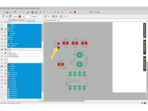
Part LED1 has no value - If I wasn't as lazy as I am, I'd have given the LED1 part a value, but until then, this warning will exist.
-
New line.Approved (0) - After you click the 'Approve' button on a warning/error, it goes in here.
-
-
-
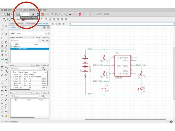
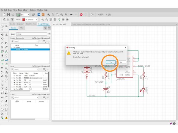
After the schematic is completed, Eagle can use your schematic information to prepare the layout procedure.
-
Click "Generate/Switch to board"
-
Click "Yes"
-
The layout editor will pop out.
-
-
-
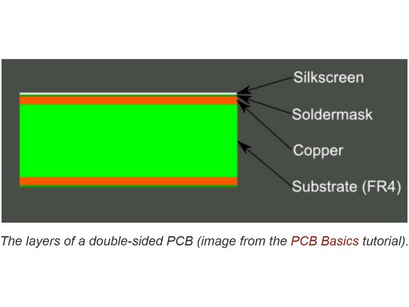
Silkscreen: This layer refers to the markings on the board that usually provides information such as component name, outlines, etc.
-
Soldermask: This is a layer of polymer that is put on a circuit board to protect the copper from oxidation and shorts during operation.
-
Copper: This is the layer where all electrical routes and vias (through holes) exist.
-
Substrate: This is a nonconductive layer that separates the top copper and bottom copper. This allows two layers of non on-overlapping routing.
-
The PCB is structured so that the above layers are sandwiched together with the substrate in the center.
-
-
-
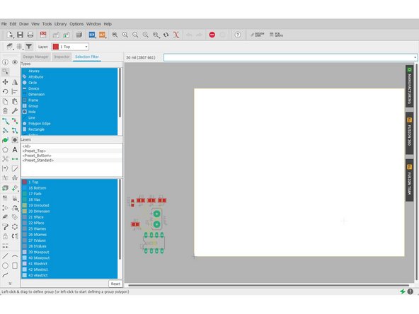
Tool Bar
-
General file control tools
-
Layer
-
Part Properties
-
Command Line
-
Layout Canvas
-
-
-
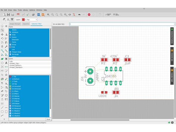
You can arrange your footprints with the:
-
Move Tool
-
Rotate Tool
-
Note that when selecting a footprint to edit, make sure you click on the cross that is in the center of the footprint.
-
-
-
Routing can be done manually or automatically.
-
You would want to route manually if there is a specific routing method you want to use.
-
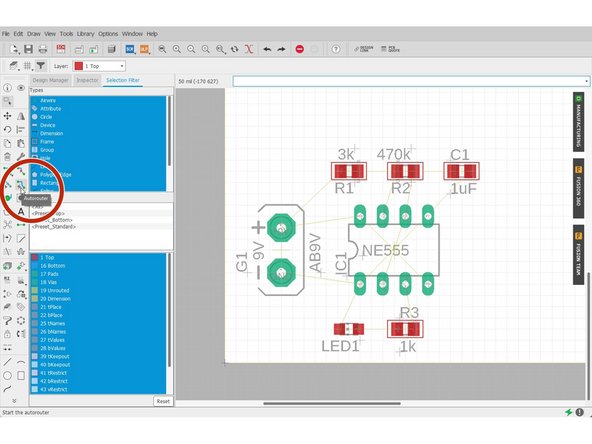
To perform automatic routing:
-
Click "Autorouter"
-
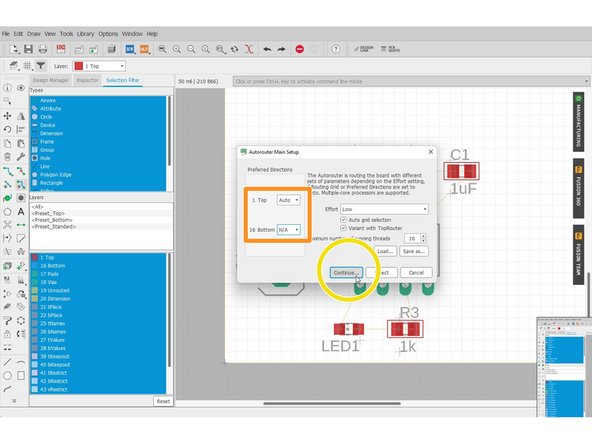
Select the board configuration for top and bottom.
-
In this example, I only want to route the top layer, so I select N/A for the bottom layer
-
Click "Continue" > "Start" > "End Job"
-
-
-
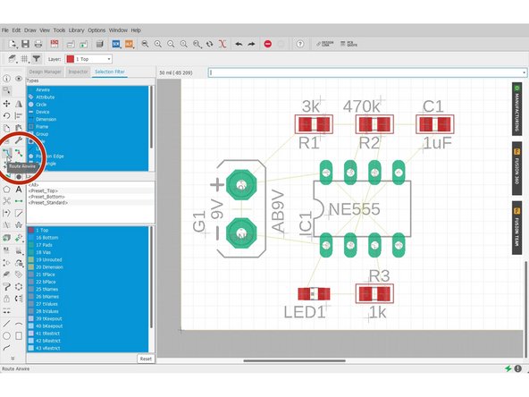
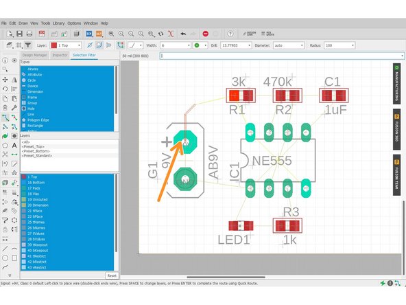
With Manual routing, you have full control over how you want to route your traces.
-
Select Route Airwire
-
Click the start of an airwire
-
Click the end of an airwire to complete a route
-
Complete by routing all the remaining airwires
-
-
-
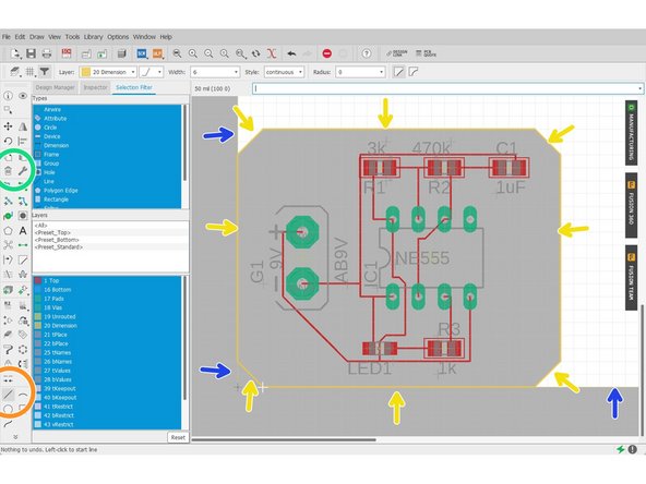
Select layer 20
-
Select Line Tool
-
Trace the board outline with the line tool
-
Select the Delete Tool
-
Remove Unnecessary lines
-
-
-
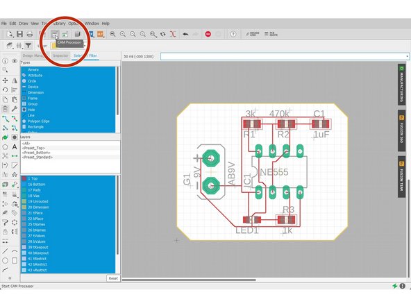
Select CAM Processor
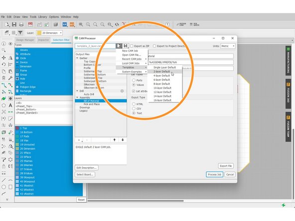
-
Select Load > Templates > 2 Layer Default
-
Or choose other templates that works best for your design
-
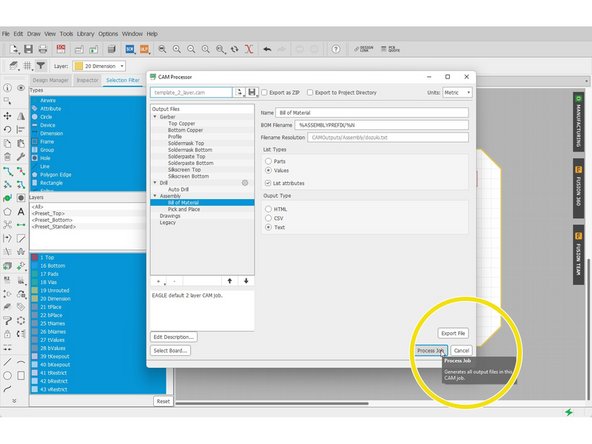
Click Process Job
-
-
-
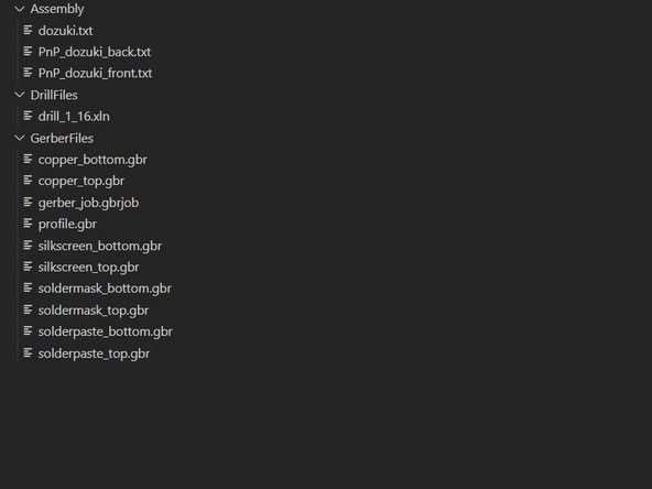
After selecting a directory to save your files in, the directory tree looks like this.
-
Congratulations! You've successfully completed a schematic design and PCB layout!
-