-
-
Altium Designer is a very very powerful circuit design, simulation, and PCB prototyping software. It is an industry standard PCB development software. Learning it now gives you an edge in internships and the real world.
-
This is the home page, it appears when you just boot Altium. A couple different things that should be pointed out, are the navigation toolbar on the left, the toolbar at the top, and the document tabs below the toolbar
-
It is important to note that the pages are highly customizable. Using the panels button in the bottom left, the properties pane, the file explorer pane, basically any pane can be removed, added, or configured. Additionally, the toolbar will change different tools depending on which stage of the process you are in.
-
You will want to double check your license. This can be done by going up to the person icon on the top right, go down to licenses, and access that page.
-
Altium works on a license basis, meaning you need to have an educational license before using it. First log in with your Altium Live account, then hit use on the license that is available
-
-
-
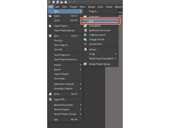
The first step to making any PCB is creating a new project. This can be done by going to the file -> new project
-
Next a Schematic document and PCB document are created within that project. This is done by going to file -> new schematic, and file -> new PCB document respectively. The fields can be filled out to your need.
-
Now you're ready to start building your PCB!
-
-
-
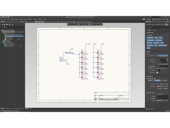
This is the schematic page. This is where the circuitry of the PCB is designed. It can be used to make the actual circuitry, wiring diagrams, and SPICE simulations.
-
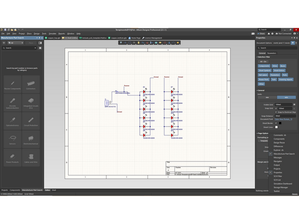
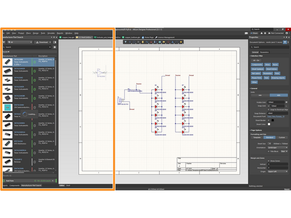
The Manufacturer Part Search(MSP) panel can be accessed in the bottom right corner of the screen where it says panels, and selecting the necessary ones. The MSP panel is the most useful panel as it allows you to put down real life components
-
Industry based components can be checked for availability and used directly
-
-
-
After making your schematic, it's time to actually design the physical PCB.
-
First you need to create a PCB doc. This can be done just like how you created the Schematic file, except instead of clicking create schematic click create PCB doc
-
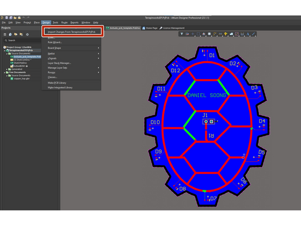
Next to import changes, navigate to the Design tool on the top left, click on Import changes from [YOUR PROJECT NAME].PrjPcb. Make sure that the schematic is within the project file first
-
You will need to hit validate and execute changes. This will use a Engineering Change Order (ECO) to pull all the components into your PCB doc
-
This will pull all the components and their necessary connections into the PCB doc for you to use.
-
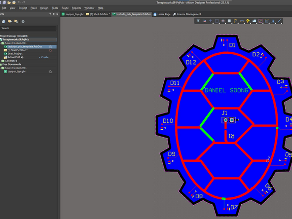
Altium is unique in allowing you to modify the PCB doc, and also being able to hit Update schematic, so you can go back and forth between the schematic and PCB document
-
-
-
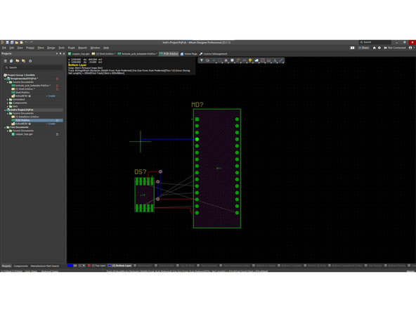
After just importing the changes form the schematic, the components will be placed in something called a room
-
The room is a pink box that is a holding area for just imported components. Take note that there are thin grey lines connecting the ends of the components to other components.
-
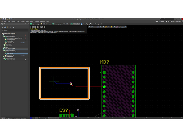
To make your PCB, drag your components over the black area. The Black represents the physical area of the PCB. Note while controlling the component, you can use space bar to rotate them.
-
To design the PCB, orient the components however you would like. Then, use the keyboard command Ctrl+W to create a trace/track. This can also be done by accessing the place tool at the top
-
Notice the cursor will snap to the pads or component connection points. Click to lay a trace down.
-
Use the keyboard command Ctrl+Shift+scroll mouse wheel while laying a trace to create a via, or to switch layers.
-
Click g to change the grid size to give more or less precision snapping to a point
-