
-
-
PCB Stands for Printed Circuit Board
-
PCBs can be imagined as a map or graph of the connections in an electric circuit.
-
A PCB is specifically printed for each circuit to make all of the necessary electrical connections
-
PCBs aren't the only way to accomplish this. The same result can be achieved with the following:
-
Solderless Breadboards
-
Prototyping Boards
-
Each of these solutions have benefits and downfalls. PCBs are the most professional and reliable solution. However, they are also less versatile, since a new circuit requires a whole new PCB to be made.
-
-
-
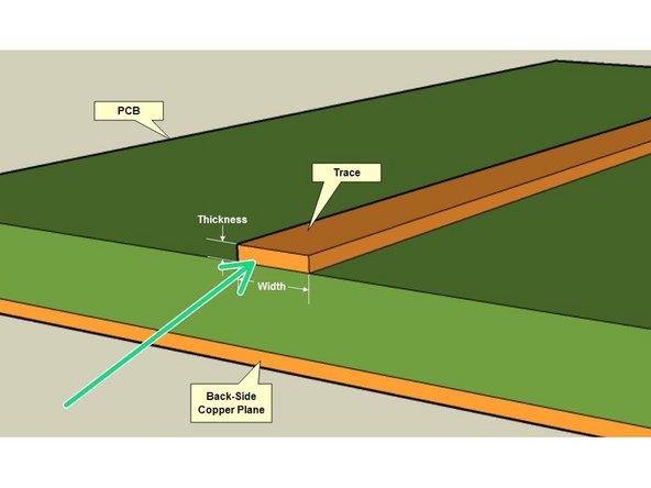
The base of a PCB is called FR-4, which is a fiberglass core with layers of copper on either side
-
This base PCB has 2 Layers. A layer is a sheet of conductive material (copper) that can carry an electric signal.
-
PCBs with more layers are created by putting alternating layers of insulator and conductor into a hydraulic press.
-
Most basic PCBs will have two layers, but more complex PCBs can have up to 10 or even more!
-
-
-
How is the electricity transmitted?
-
As we saw, each layer can transmit a signal across it. However, we still need a way to transmit a signal across layers and to place multiple signals onto a single layer.
-
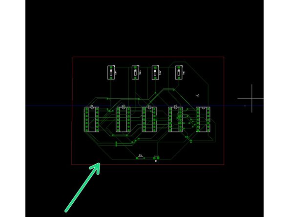
Traces: Thin strips of copper on a layer of the PCB. These link components on the same layer of the PCB.
-
Conductive material left over after a PCB layer has been milled out.
-
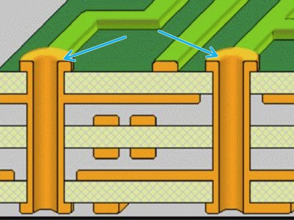
Vias: These are small holes that transmit a signal across different layers on the PCB
-
Small holes that are drilled out and then electroplated with a conductor
-
Through-Holes: Holes where components are soldered in. The solder electrically connects all of the layers that it passes through.
-
Large holes that are drilled out and the electroplated with a conductor
-
-
-
Components are any electrical devices that will be directly connected to a PCB. There is an incredibly varied selection of components that can be used, but they fall into two main categories:
-
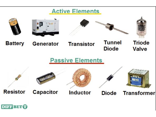
Active Circuit Elements: Small chips with multiple input and output pins to interface with the circuit inside. Includes logic gates, op-amps, ROMs, microprocessors, and more
-
Passive Circuit Elements: These are components with two terminals with specific electrical properties like a resistor, inductor, capacitor, or diode
-
These groups are a huge simplification of the components that can actually be on a PCB, but they provide a wide foundation. Don't feel constrained by these groups if you are looking to create a PCB.
-
On a PCB, there can be hundreds or even thousands of connections. When circuits get this large, a PCB is the best way to package them
-
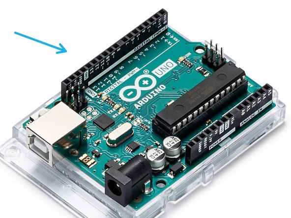
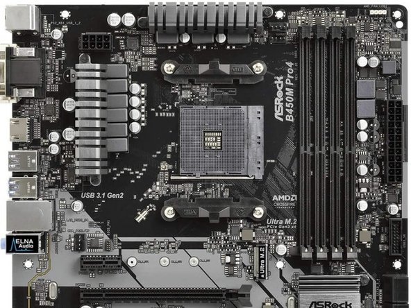
Try to spot some of the different Passive and Active circuit elements on the Arduino and Motherboard
-
-
-
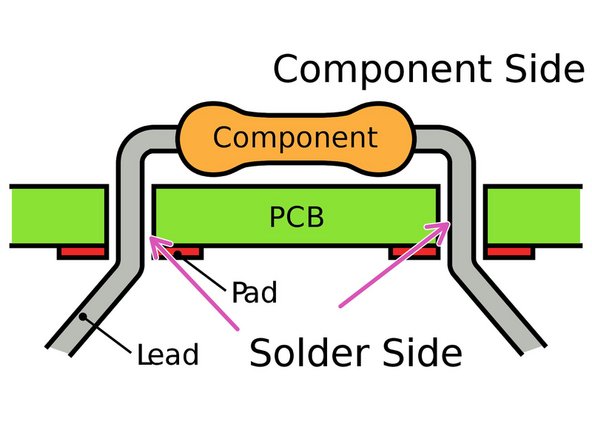
Surface-Mount footprints (SMD) consist of solder "pads", which are small, flat, exposed pieces of copper that components can be soldered onto
-
Soldered with solder paste and a reflow oven
-
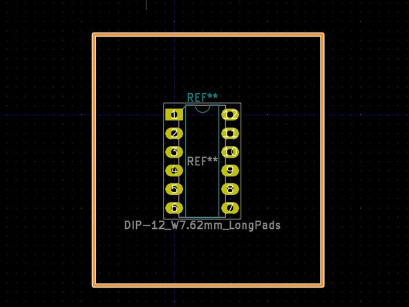
Through-Hole (THT) footprints consist of through-holes that go all the way through the PCB
-
Soldered with wire solder and a soldering iron
-
Why choose one component type over the other?
-
SMD components are significantly more compact and allow for more complex PCBs to be made smaller. However, they are also more difficult to solder and require specialized equipment
-
THT components are large and connect to all layers of a multi-layer PCB. This makes them worse for creating more compact PCBs, but are still a good option for larger components like connectors and pinouts
-
-
-
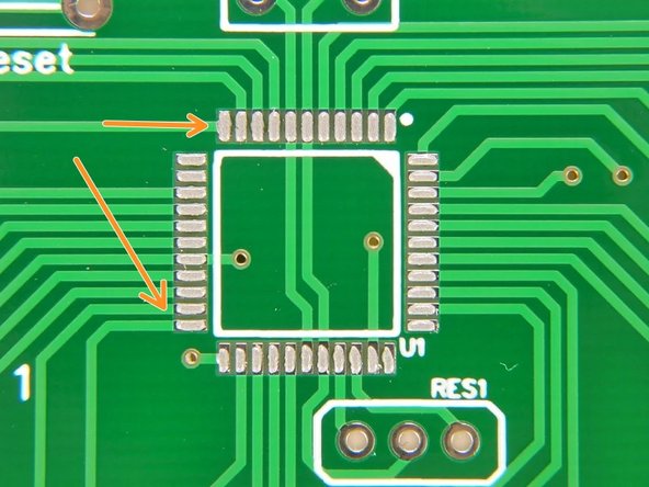
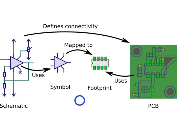
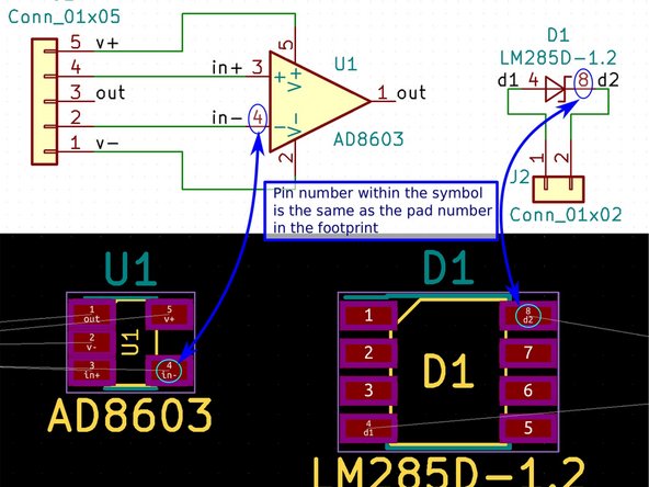
A PCB interacts with a component through its Footprint.
-
A footprint maps the schematic symbol to the physical solder pads and through-holes that it will use to interact with the PCB
-
Active Components usually have footprints that consist of connections arranged in an array to interface with the circuit inside
-
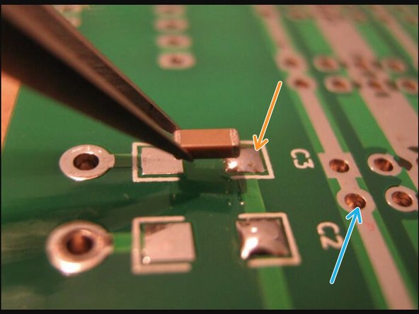
Passive Elements typically have less complex footprints with 2-3 connections.
-
Both types of components can use SMD or THT mounting. The footprints will be different for the SMD and THT versions of the same device.
-
Footprints can also change based on the component's size. SMD components, in particular, have many different sizes for the same components.
-
-
-
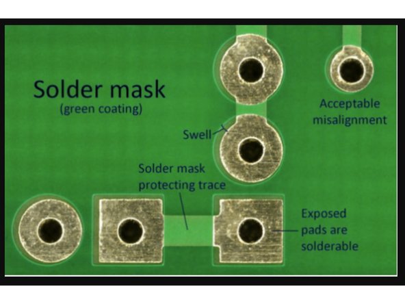
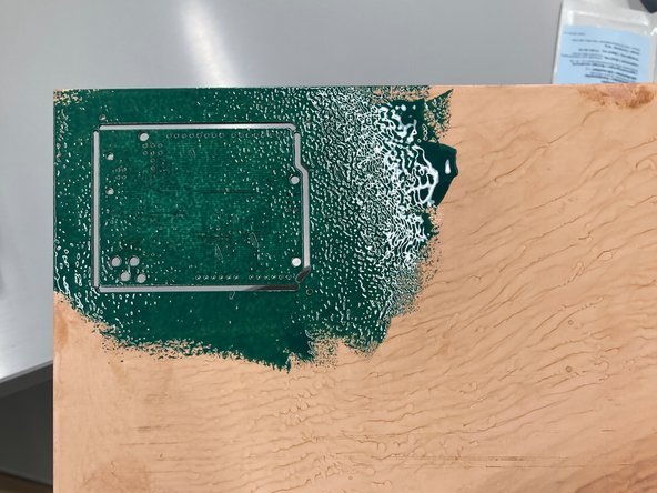
During production, PCBs are covered with a layer of "Solder Mask," which is a green polymer coating that:
-
Repels Solder
-
Solder is made to stick to exposed metal, which improves it's electrical connection to a circuit. However, we only want solder on the solder pads. Therefore, Solder mask is made to repel solder to ensure that it doesn't stick and conduct anywhere that we don't want it to.
-
Removes Conductivity
-
The outer surface of a PCB is conductive without solder mask. If two unprotected PCBs touch, they could interfere with each other's operation.
-
Protects the Top and Bottom Surfaces
-
The outer surface of a PCB is just a sheet of copper. If this gets scratched or damaged, it can interfere with the signal quality.
-
-
-
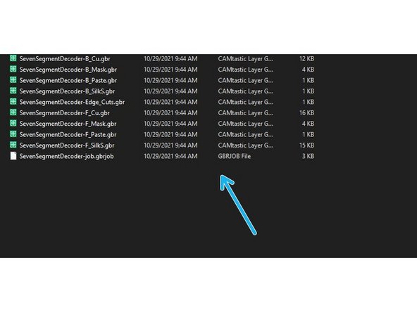
PCBs are exported and created using Gerber files (.gbr or .gb)
-
These files contain many different layers, each representing one part of the PCB
-
Some examples are: top copper, bottom copper, drill holes, silkscreen, and solder mask
-
These files are given to complex machinery that reads them and does the processing necessary to create the finished PCB
-
The process is a collection of drilling, milling, and electroplating steps, which you will learn about in a future guide
-


Cancel: I did not complete this guide.
10 other people completed this guide.