
Introduction
This guide gives a primer on special considerations for using an SEM to characterize Nanoscribe prints. This guide is aimed at those already trained on an SEM through either the Fablab or the AIM lab or who consider themselves intermediate users with a different facility. This guide first covers the major aberrations and artifacts expected from Nanoscribe parts, then details a few approaches to correcting or avoiding them. If none of the suggested fixes are available on your SEM, let us know in the comments so we can update the guide.
-
-
The Nanoscribe prints on three possible substrates: borosilicate glass, glass coated in ITO, or undoped silicon wafer in the <100> direction
-
The success of scanning electron microscopy depends, in part, on the conductivity of sample. Insulating materials collect surface charge and produce aberrations as a result.
-
Borosilicate Glass: insulating
-
ITO Coated Glass: Top surface coated in ITO conductive
-
Si wafer: Conductive enough to prevent charging
-
-
-
Though some of the substrates are conductive, all of the material deposited by the Nanoscribe is not
-
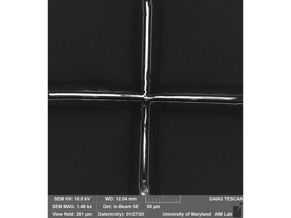
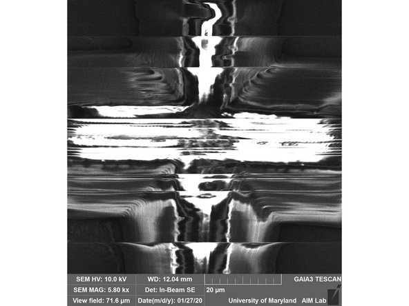
The insulating print gathers charge under an electron beam. The resulting electric field warps the trajectory of the secondary electrons, producing the sort of aberrations pictured here
-
Charging aberrations arise in secondary electron imaging mode
-
Especially evident at higher magnifications
-
-
-
The image on this step shows charging with non-physically bright regions
-
This image also indicates a significant astigmatism as one line is blurrier than its perpendicular counterpart
-
Charging aberrations make correcting astigmatism by adjusting stigmators more difficult
-
-
-
Solves charging problem
-
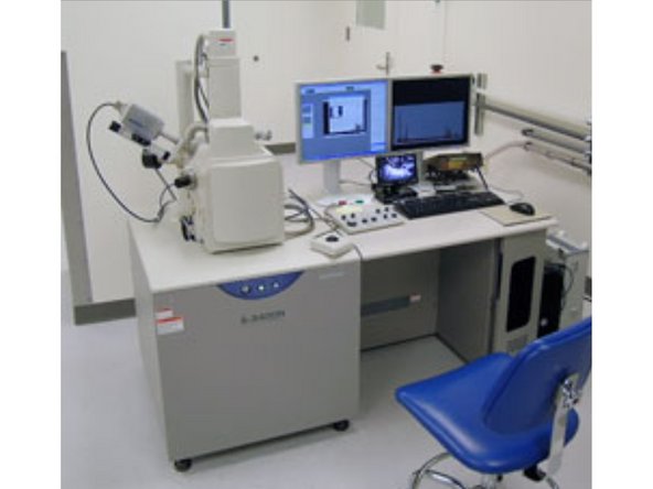
If you have training and access to a variable pressure SEM, performing measurements in environmental mode reduces charging
-
The Hitachi S-3400 Variable Pressure SEM in the FabLab can image in this mode
-
If this is an option, try this first
-
-
-
Imaging mode not subject to charging aberration
-
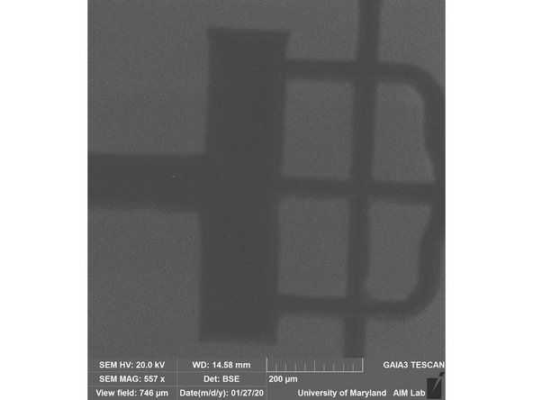
Backscatter electron (BSE) trajectories are deviated less than secondary electrons by a surface charge, so this imaging mode is not vulnerable to charging aberrations
-
First image taken in BSE mode, second image taken in SE mode
-
Contrast in BSE stems from atomic weight, so BSE images do not show topology features
-
This is also a good option to avoid charging aberrations
-
-
-
SEM samples are conventionally mounted to aluminum stubs with carbon or copper tape. For samples printed on ITO-coated slides, wrap the tape around to the front of the slide to insure a conductive pathway from the ITO to the aluminum stub
-
Where possible, use a lower beam power. A lower power reduces the amount of charging, though not to the point of eliminating the aberration.
-
Perform the initial alignment in BSE mode
-
I cannot stress enough how valuable environmental mode is for microanalysis of Nanoscribe prints
-

Cancel: I did not complete this guide.
One other person completed this guide.