
Introduction
This guide is the first in a series of guides that will show users how to use the LPKF machines located in the Electronics Prototyping (EP) space of the Advanced Fabrication Lab (AFL). They will cover everything from basic circuit technologies to the intricacies of manufacturing circuit boards. These guides assume a background in electronics. Circuit theory and PCB design are outside the scope of these guides, they purely focus on PCB manufacturing.
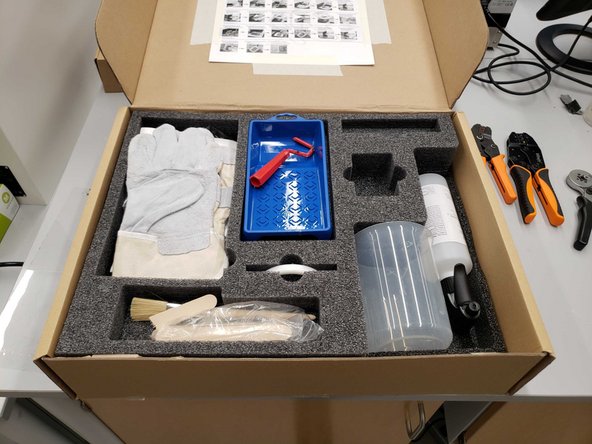
Parts
No parts specified.
-
-
The basic process for making a double layer PCB is as follows:
-
Drill all the vias (holes) in the board.
-
Plate the insides of the vias.
-
Route all the traces (wires).
-
Apply solder mask to insulate the board and silkscreen to add text.
-
Solder components onto the board
-
-
-
Several materials can be used to make circuit boards. They offer different thicknesses and properties such as being flexible.
-
FR4 is the most common material. It is a composite material composed of woven fiberglass cloth with an epoxy resin binder that is flame resistant.
-
Two thin layers of copper foil are attached to either side to make PCB fabrication possible.
-
FR4 comes with different widths, lengths, thicknesses, and amount of copper.
-
-
-
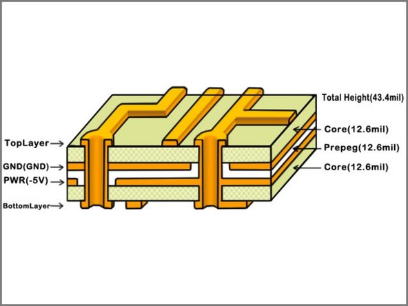
PCBs are comprised of multiple layers.
-
The LPKF machines are capable of making up to 8 layer circuits.
-
Most common is 2 layers (front and back of a sheet of FR4).
-
-
-
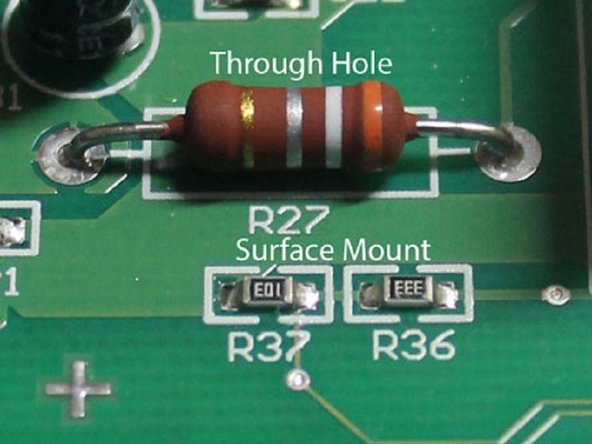
2 most common are surface mount and through hole.
-
Through hole components have pins that stick through the PCB.
-
Through hole is much easier to solder by hand.
-
SMD components (Surface Mount Devices) sit on the surface of the board on copper pads.
-
Surface mount devices are much harder to hand solder.
-
Surface mount components are measured in sizes ranging from 0201-2512 with 0805 being one of the most common.
-
-
-
The ProtoMat S64 routes traces and drills holes.
-
Stencils for applying solder paste are also made on the S64.
-
-
-
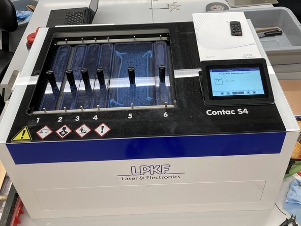
The Contac S4 uses electrolysis to copper plate the insides of the vias.
-
This allows the vias to electrically connect the top layer to the bottom layer.
-
On 2 layer boards it is used between drilling vias and routing tracks.
-
-
-
The ProMask kit is used to apply solder mask (green) on circuit boards.
-
The solder mask repels solder and insulates the board.
-
It protects the board and ensures solder goes where it needs to go.
-
-
-
The ProLegend kit comes in the same box as the ProMask kit and is used to apply silkscreen (white) to the board.
-
The silkscreen layer contains all the text and markings on the board.
-
You can add text and graphics to label components or add your logo.
-
-
-
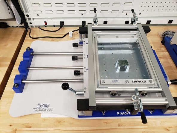
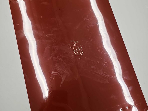
The ProtoPrint is the mount used to spread solder paste on the boards.
-
A stencil is used to place solder paste on the pads of the board.
-
Stencils get routed out on the ProtoMat S64 and then are placed in a frame.
-
The PCB is placed under the stencil.
-
Solder paste is spread over the stencil with a tool and is neatly deposited onto the pads of the PCB.
-
-
-
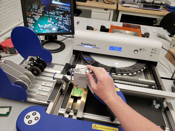
The ProtoPlace uses compressed air to place components onto a PCB.
-
The user picks up components with a pressurized needle and places them on the board with the help of a monitor and fine adjustment knobs.
-
-
-
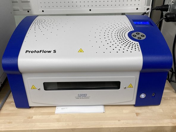
The ProtoFlow is a reflow oven that follows specific temperature curves to melt solder paste and cure solder mask/silkscreen.
-
-
-
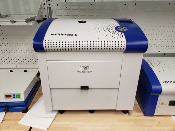
The MultiPress S is used to create multi-layer boards.
-
Additional sheets of copper foils are pressed onto a sheet of FR4.
-
PCBs can have up to 8 layers with this machine.
-
-
-
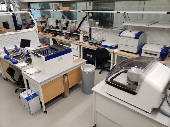
The overall procure to make a PCB takes about two days and requires the use of several specialized machines.
-
As well as the LPKF equipment in the EP there are two workbenches with basic electronics equipment.
-


Congratulation! You now know the general process behind making PCBs. Each machine has its own guide which will go more in-depth with how to use it. Feel free to reference this guide or click on any of the machines listed as tools on the top if you need any refreshers.
Congratulation! You now know the general process behind making PCBs. Each machine has its own guide which will go more in-depth with how to use it. Feel free to reference this guide or click on any of the machines listed as tools on the top if you need any refreshers.
Cancel: I did not complete this guide.
17 other people completed this guide.